Leaderboard


Popular Content
Showing content with the highest reputation on 01/27/13 in all areas
-
Asrock already killed that link And series 6 chipsets killed off BSEL and VID mods. VID is now controlled through 1 single pin with a serial data format instead of the old multiple pins with fixed voltages. BSEL mods are also dead since regular sandy bridge has no option for a BCLK other than 100MHz (SB-E does, but it's on a much different socket), so even if there were still BSEL pins, there would be nothing to select between. And if paying for an i5 is a problem, you probably shouldn't mess around with fuses on your i3 to try to get a higher multiplier since there's a good chance you'll kill it, and you would need to buy a higher clocked CPU to compare against. On a side note, I do have the same i3 that you have and a 2920xm ES. I'm thinking that the 3 rows of circular contact pads are where intel applied current to blow the fuses. There's probably a coating over them that needs to be sanded off to test resistances. I'm really not interested in sanding the 2920 since it's unlocked anyway, so I doubt I'll pursue this. It would be better to have the next speed bin up i3 to compare against to try to isolate the multiplier fuses. I wonder if CPUID extensions are also set through fuses? Intel has to set them somehow, and I don't think CPUs have flash memory on them. This would be interesting since then you could not only enable a higher multiplier, but set it as well without having to hack the BIOS and ME FW. I am willing to sand and test the contacts on an i3-2310m (2.1GHz) if anyone has a similar CPU such as an i3-2330m (2.2GHz) that they are also willing to sand and compare with. The idea would be to find 2 contacts that are connected on the 2330m, while the same contacts have no connection on a 2310m, meaning that the fuse between those contacts on the 2310m had been blown. I'm thinking that the 80 contacts are likely routed to VCC or GND, not each other. Below is what I'm guessing is the fuse setup: Inside the CPU die: The CPU reads high or low voltage from a contact pad on the gate of a transistor. This gate is connected to VCC through a pull-up resistor (resistors are doable on a CMOS process). Outside the CPU die: 80 lines from the CPU die go out directly to the 80 contacts in the 3 rows. The contact pads are also individually routed to GND through their own fuse. How it works: When a fuse is not blown, the voltage drop from VCC to GND will occur across the internal pull-up resistor on the CPU die, and thus the voltage on the gate is GND. When a fuse is blown, there is no connection to GND at all, and the gate will be pulled up to VCC through the internal resistor on the CPU die. There will be no voltage drop across the resistor because CMOS gates block all current. To blow a fuse, Intel applies a voltage to the contact pad. Since there is no resistor between the contact pad, the fuse, and GND, the fuse will blow, and the CPU die is unharmed as long as the voltage isn't too far above normal VCC. In the scenario above, VCC and GND could be swapped, but the concept is identical. A more complicated method where any of the 80 contacts can be connected together I think is highly unlikely. It would be a more costly method since it requires twice the amount of contact pads, and there would still need to be a direct VCC or GND connection anyway for the CPU to read the fuse state without possibly seeing a floating voltage. This is good for us, since it means that we just have to test the resistance between the pads and VCC or GND, which can easily be found on the socket pins on the other side of the CPU package, or any other contact with a non-blown fuse. The main danger is the multimeter resistance reading circuit being too capacitive, which could blow fuses if the multimeter lead floats significantly apart from the voltage on the pad before reading the resistance. The fuse should be safe as long as the other lead is connected to GND (or VCC) first, and the multimeter is set to reading resistance before contacting the pad. For complete safety a resistor could be added in series between the multimeter and the CPU. This will make sure current doesn't flow too quickly in case the multimeter is floating significantly. An intact fuse should have no readable resistance, so you'll only see the resistance of the added resistor. I might test out this theory on my spare i3, make up a diagram, and start a new thread looking for volunteers. Will probably be a few weeks before I do though.2 points
-
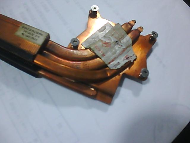
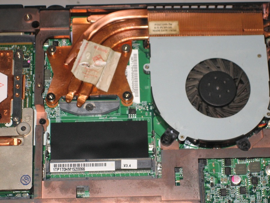
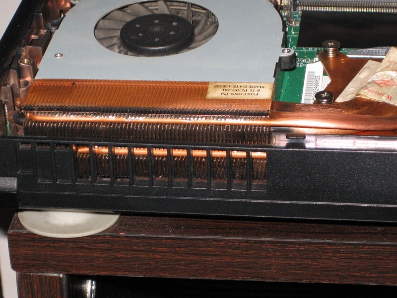
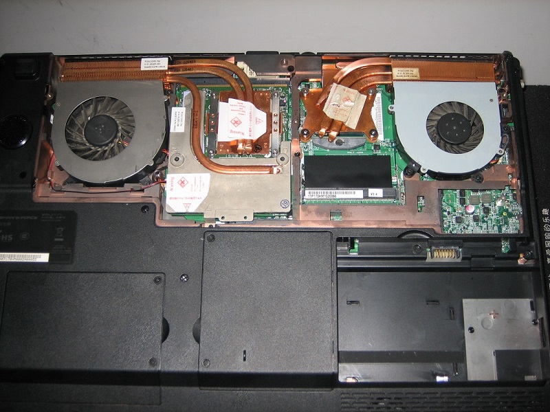
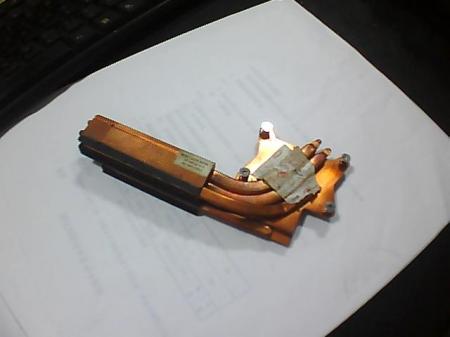
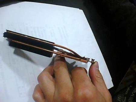
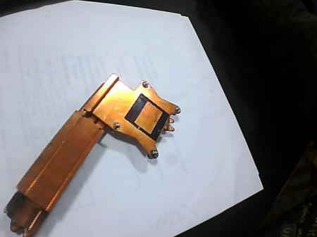
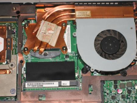
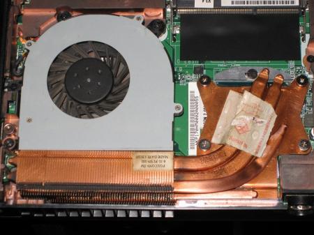
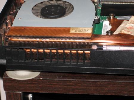
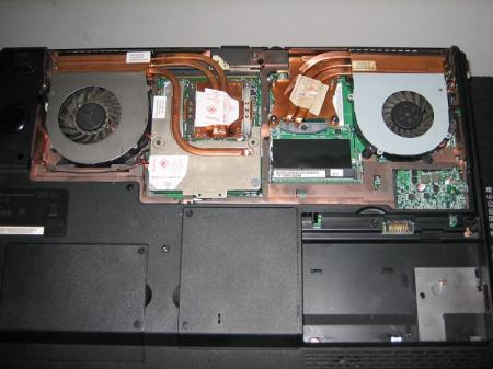
Transformation of the CPU cooling module


 1 point
 -
Try to unplug the psu and the battery of your laptop, then push the power on button (to discharge the condensator) ... after that, plug your battery and try to power on your laptop. Your laptop is shutting down due to an overload on your PSU (if you have a 180W PSU don't try ov superior to 1v, the 1v overvolt can overload your psu in certain circumstance, so ov superior to 1v could damage your PSU) If you have a 180W PSU buy a wattmeter to measure the consumption at the outlet.1 point
-
Hi, I came here from NBR (got the same name so some might recognize me) I got interested in computers when i bought my MSI GE60. I have been overclocking it for a bit but want to take it to the next level (currently got the highest 3dmark vantage score for i5 and 650m) So i signed up here to learn about advanced overclocking I heared at NBR this was the place to learn about tweaking the vbios and stuff like that. Cheers, Daniel1 point
-
Hi I use 310.90 but the shutdown is not driver related. you are right your 180W psu is overloaded, so the laptop shutdown to prevent damage. I have got the same problem with MSI ov 1v but only with Far Cry 3, i record a peak @ 200w, which is huge for a 180w psu. I decide to flash the card with msi 80.04.33.00.24 oc edition with stock voltage (0.987v) and oc to a max 980/2400. You won't notice a huge difference in game (only 20mhz less - 1 or 3 fps less). Yes the msi fd bios works with P150HM, but they are less stables than the msi final (sometimes the card stay at idle clock when you launch 3d app). You can try this one : http://forum.techinferno.com/general-notebook-discussions/2062-using-your-4gb-gtx-680m-its-safest-full-potential.html But it's also a 1v ov so i think it will overload your psu too. Good luck1 point
-
@MSI users: I just added fixed versions for the MSI vbios mods to the second post. The overvolts should now work properly, and the normal 'OCedition' (the not overvolted one) now runs at 0.987v instead of 1.012v. This will result in a cooler running card without loosing any stability. Default clock is still at MSI setting, 771MHz. Forget about the turbo button on your systems, those vbios run at 771MHz when not overclocked. It's uefi compatible, and the whole vbios is completely revised.1 point