
Leaderboard


Popular Content
Showing content with the highest reputation on 03/28/12 in all areas
-
This is a modified version of BIOS A10, with all the hidden menus made available. The archive with the BIOS and the necessary files to flash it are attached to the post. After flashing, go to the BIOS menu and load the default settings, save, exit and reboot. As always with such modifications, you alone are responsible for your system and what you do with it. If you flash it, please report back and let me know whether everything is ok. (I'm sure it is, but I don't have an M17x R3 myself to test it ) The menus look exactly the same as all the previous "unlocked" R3 BIOS versions. Tested and confirmed to work, thanks @Staff Sargent !! *********************************************** Please consider a donation if you like this modified BIOS. *********************************************** UPDATE: Had to correct some things, this works fine. Keep in mind that A10 is no longer officially available on Dells support site, I don't know the reason for this, they might have to fix some things. Update 2: BIOS is available again on Dell's site, nothing changed between the version which was on there earlier and now... lol. M17x R3 - [unlocked] BIOS A10.zip4 points
-
Fresh drivers are out. Please report your findings in case you install them. Release notes: Catalyst Software Suite 12.3 - direct download (Win7 64bit) AMD site - CCC 12.3 No new CAP so far, latest official is still 12.2 CAP13 points
-
here you go check this one to get used to the normal bios options and descriptions with pics http://forum.techinferno.com/alienware-m18x/1054-alienware-m18x-stock-bios-xm-guide.html after reading that thread go here and read though... ignore anything directly referencing using the hexeditor to mod the bios all other content in this thread is related to our M18x unlocked bios and has pics for you. http://forum.techinferno.com/alienware-m18x/1125-m18x-a03-bios-modifying-via-da_gs-method-hex-registers-editing.html#post13085 after that please mention or quote me and i'll be more than glad to help you set up from there. here i have post on common voltages needed for what cpu frequencies. and thats located in this thread here http://forum.techinferno.com/alienware-m18x/1491-2920xm-overclocking-guide-detailed-results.html any questions we will be glad to help. @svl7 thank you for covering that question.1 point
-
Hi and welcome to T|I! Don't worry, the thread isn't dead, this is the number one source for modded M18x BIOS I can't remember whether there have been screenshots of the menus somewhere on the forum, but you can find -2.html#post10874"]screenshots of the unlocked menus of the M17x R3 BIOS here, should be pretty much the same as in the M18x. Of course if you have an XM CPU in the M18x, you'll see the advanced CPU overclocking options in addition to this, but that's independent of whether the BIOS is unlocked or not. Hope this helps.1 point
-
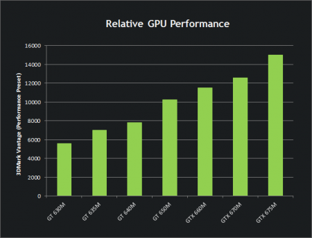
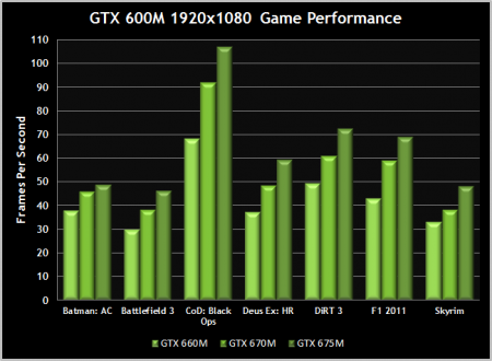
So... after months of wild speculating and guessing we finally have some first official numbers regarding the new mobile GPUs of Nvidia. Here the specifications listed on the official Nvidia site: GTX 660M GTX 670M GTX 675M Graphics Clock 835MHz 598MHz 620MHz CUDA Cores 384 336 384 Texture Fill Rate (billion/sec) 30.4 33.5 39.7 Memory Interface DDR3/GDDR5 DDR3/GDDR5 DDR3/GDDR5 Memory Clock 2000MHz 1500MHz 1500MHz Memory Interface Width 128-bit 192-bit 256-bit Memory Bandwidth (GB/sec) 64 72 96 Max SLI Configuration 2-Way 2-Way 2-Way 610M GT 620M GT 630M GT 635M GT 640M LE GT 640M GT 650M Graphics Clock 900MHz 625MHz 800MHz 675MHz 500MHz 625MHz 850MHz CUDA Cores 48 96 96 144 384 384 384 Texture Fill Rate (billion/sec) 7.2 10 12.8 16.2 16 20 27.2 Memory Interface DDR3 DDR3 DDR3/GDDR5 DDR3 DDR3/GDDR5 DDR3/GDDR5 DDR3/GDDR5 Memory Interface Width 64-bit 128-bit 128-bit 192-bit 128-bit 128-bit 128-bit Memory Bandwidth (GB/sec) 14.4 28.8 32 43.2 28.8 64 64 There are seven 600m series GPUs which can be considered low- to middle-end and three which are high-end.No word on the Nvidia site about which manufacturing process is being used for these chips, but the statement telling one should assume that they really shifted to 28nm only, but I want to see this confirmed before I really believe this to be true.Anyway, looking at the specs of Nvidias new mobile flagship, the GTX 675m I can't help but to think that they just shrinked the fermi architecture... the specs and clocks are identical to the 580m. They might also have messed up the numbers they put on the site, it just seems unlikely that all GPUs from the 640m up to the 675m all have the same core count (except for the 670m).Well, I guess we will see more information in the near future, when the first systems with these GPUs are getting released. I'm definitely curious about how they perform and can't wait to see some benchmarks. Also the overclocking capability is going to be a very interesting point. So far there's no word about new features for this GPU series, so it's unclear whether the "clock boost" technology which can be found in the desktop GTX 680 will also make its way to the mobile GPUs. Here some performance graphs, also taken from Nvidias website:[ATTACH=CONFIG]3707[/ATTACH] [ATTACH=CONFIG]3708[/ATTACH] So far I'm really not that impressed, though we have yet to see the real world performance, and tbh I'm really curious about the AMD 7000m series :)
 1 point
 -
Next BF3 Patch: (Release: around 27.03.2012)1 point
-
1 point

