

Xtof
-
Posts
11 -
Joined
-
Last visited
Xtof's Achievements
Settling In (2/7)
11
Reputation
-
Well, PLL is detected now thanks to the following kernel parameter: acpi_enforce_resources=laxNow, I have a newly detected i2c-7 device. As expected, the PLL is at the 0x69 adress : # i2cdetect -l i2c-0 i2c i915 gmbus ssc I2C adapter i2c-1 i2c i915 gmbus vga I2C adapter i2c-2 i2c i915 gmbus panel I2C adapter i2c-3 i2c i915 gmbus dpc I2C adapter i2c-4 i2c i915 gmbus dpb I2C adapter i2c-5 i2c i915 gmbus dpd I2C adapter i2c-6 i2c DPDDC-D I2C adapter i2c-7 smbus SMBus I801 adapter at ef80 SMBus adapter# i2cdetect -y 7 0 1 2 3 4 5 6 7 8 9 a b c d e f 00: -- -- -- -- -- 08 -- -- -- -- -- -- --10: -- -- -- -- -- -- -- -- -- -- -- -- -- 1d -- --20: -- -- -- -- -- -- -- -- -- -- -- -- -- -- 2e --30: -- -- -- -- -- -- -- -- -- -- -- -- -- -- -- --40: -- -- -- -- 44 -- -- -- -- -- -- -- -- -- -- --50: UU -- UU -- -- -- -- -- -- -- -- -- -- -- -- --60: -- -- -- -- -- -- -- -- -- 69 -- -- -- -- -- --70: -- -- -- -- -- -- -- --When I check the PLL registers, I can confirm it is really TME-unlocked (see 26 (=#00100110b) at 0x9 offset) # i2cdump -y 7 0x69 s 0 0 1 2 3 4 5 6 7 8 9 a b c d e f 0123456789abcdef 00: 51 aa ff ef ff dc 80 31 58 26 01 05 0d Q?.?.??1X&???But overclocking using lfsb tool still not work. I think it tries to write to the wrong i2c device. Now, I have to check the source code to understand how it works. # /usr/local/bin/lfsb/./lfsb-x64 -y ics9lprs397 266 ------------------------------------------------------------- CPU frequency : 1060.04 MHz (estimated) PLL ics9lprs397 is supported. ------------------------------------------------------------- Changing to: FSB=266 MHz Can't change frequency, SetFSB error: No such device or address ------------------------------------------------------------- CPU frequency : 1108.91 MHz (estimated) FSB=266 MHz -------------------------------------------------------------
-
Yesterday, the computer was upgraded with ubuntu gnome 14.04 Still the same issue, the PLL seems not detected under linux. The command i2cdetect -l gives the following result : # i2cdetect -l i2c-0 i2c i915 gmbus ssc I2C adapter i2c-1 i2c i915 gmbus vga I2C adapter i2c-2 i2c i915 gmbus panel I2C adapter i2c-3 i2c i915 gmbus dpc I2C adapter i2c-4 i2c i915 gmbus dpb I2C adapter i2c-5 i2c i915 gmbus dpd I2C adapter i2c-6 i2c DPDDC-D I2C adapter
-
The hardmod BSEL=266Mhz (with also TME unlocked) works very well without doing anything else than soldering. The CPU runs at 1.6 GHz without any effort but the lowest speed has increased from 800 MHz to 1.06 GHz. If I understand well, the 2nd solution may allow the CPU to run at a 266MHz FSB while being detected as 200 MHz by the CPU, which then may allow me to keep the x7 multiplier ? I think I miss something in your last sentence, I don't understand why it is usefull to downclock the RAM if I know it supports 266 MHz FSB (its PC2-6400). I disabled the red pinmod to focus on TME-unlock only. Well, this time I haven't any success up to now. Still investigating but it seems that the PLL is not detected on the i2c bus. I use Ubuntu gnome 13.04 and the dual-IDA modded bios. Here is what I have done, getting inspiration from this link (I verified that the correct register was still #FED1F418h with U9x00 CPU. I also verified its default value at startup in grub = #3380009h) : 1. Activate smbus in /boot/grub/grub.cfg by adding write_dword 0xFED1F418 0x3380001 2. I checked it is activated using # lspci | grep -i smbus 00:1f.3 SMBus: Intel Corporation 82801I (ICH9 Family) SMBus Controller (rev 03) 3. Installed drivers for smbus # modprobe i2c_dev # modprobe i2c_i801 4. Installed the archive containing lfsb in /usr/local/bin # /usr/local/bin/lfsb/./lfsb-x64 -y ics9lprs397 266 ------------------------------------------------------------- CPU frequency : 399.63 MHz (estimated) PLL ics9lprs397 is supported. ------------------------------------------------------------- Changing to: FSB=266 MHz Can't change frequency, SetFSB error: No such device or address ------------------------------------------------------------- CPU frequency : 344.74 MHz (estimated) FSB=266 MHz ------------------------------------------------------------ It seems impossible to change FSB. 5. The command ls /dev/i2c* list all devices on i2c bus : # ls /dev/i2c* /dev/i2c-0 /dev/i2c-1 /dev/i2c-2 /dev/i2c-3 /dev/i2c-4 /dev/i2c-5 /dev/i2c-6 When I scan devices in the i2c bus : # i2cdetect -y 0 0 1 2 3 4 5 6 7 8 9 a b c d e f 00: -- -- -- -- -- -- -- -- -- -- -- -- -- 10: -- -- -- -- -- -- -- -- -- -- -- -- -- -- -- -- 20: -- -- -- -- -- -- -- -- -- -- -- -- -- -- -- -- 30: -- -- -- -- -- -- -- -- -- -- -- -- -- -- -- -- 40: -- -- -- -- -- -- -- -- -- -- -- -- -- -- -- -- 50: -- -- -- -- -- -- -- -- -- -- -- -- -- -- -- -- 60: -- -- -- -- -- -- -- -- -- -- -- -- -- -- -- -- 70: -- -- -- -- -- -- -- -- # i2cdetect -y 1 0 1 2 3 4 5 6 7 8 9 a b c d e f 00: -- -- -- -- -- -- -- -- -- -- -- -- -- 10: -- -- -- -- -- -- -- -- -- -- -- -- -- -- -- -- 20: -- -- -- -- -- -- -- -- -- -- -- -- -- -- -- -- 30: -- -- -- -- -- -- -- 37 -- -- -- -- -- -- -- -- 40: -- -- -- -- -- -- -- -- -- 49 -- -- -- -- -- -- 50: 50 -- -- -- -- -- -- -- -- 59 -- -- -- -- -- -- 60: -- -- -- -- -- -- -- -- -- -- -- -- -- -- -- -- 70: -- -- -- -- -- -- -- -- # i2cdetect -y 2 0 1 2 3 4 5 6 7 8 9 a b c d e f 00: -- -- -- -- -- -- -- -- -- -- -- -- -- 10: -- -- -- -- -- -- -- -- -- -- -- -- -- -- -- -- 20: -- -- -- -- -- -- -- -- -- -- -- -- -- -- -- -- 30: -- -- -- -- -- -- -- -- -- -- -- -- -- -- -- -- 40: -- -- -- -- -- -- -- -- -- -- -- -- -- -- -- -- 50: 50 -- -- -- -- -- -- -- -- -- -- -- -- -- -- -- 60: -- -- -- -- -- -- -- -- -- -- -- -- -- -- -- -- 70: -- -- -- -- -- -- -- -- # i2cdetect -y 3 0 1 2 3 4 5 6 7 8 9 a b c d e f 00: -- -- -- -- -- -- -- -- -- -- -- -- -- 10: -- -- -- -- -- -- -- -- -- -- -- -- -- -- -- -- 20: -- -- -- -- -- -- -- -- -- -- -- -- -- -- -- -- 30: -- -- -- -- -- -- -- -- -- -- -- -- -- -- -- -- 40: -- -- -- -- -- -- -- -- -- -- -- -- -- -- -- -- 50: -- -- -- -- -- -- -- -- -- -- -- -- -- -- -- -- 60: -- -- -- -- -- -- -- -- -- -- -- -- -- -- -- -- 70: -- -- -- -- -- -- -- -- # i2cdetect -y 4 0 1 2 3 4 5 6 7 8 9 a b c d e f 00: -- -- -- -- -- -- -- -- -- -- -- -- -- 10: -- -- -- -- -- -- -- -- -- -- -- -- -- -- -- -- 20: -- -- -- -- -- -- -- -- -- -- -- -- -- -- -- -- 30: -- -- -- -- -- -- -- -- -- -- -- -- -- -- -- -- 40: -- -- -- -- -- -- -- -- -- -- -- -- -- -- -- -- 50: -- -- -- -- -- -- -- -- -- -- -- -- -- -- -- -- 60: -- -- -- -- -- -- -- -- -- -- -- -- -- -- -- -- 70: -- -- -- -- -- -- -- -- # i2cdetect -y 5 0 1 2 3 4 5 6 7 8 9 a b c d e f 00: -- -- -- -- -- -- -- -- -- -- -- -- -- 10: -- -- -- -- -- -- -- -- -- -- -- -- -- -- -- -- 20: -- -- -- -- -- -- -- -- -- -- -- -- -- -- -- -- 30: -- -- -- -- -- -- -- -- -- -- -- -- -- -- -- -- 40: -- -- -- -- -- -- -- -- -- -- -- -- -- -- -- -- 50: -- -- -- -- -- -- -- -- -- -- -- -- -- -- -- -- 60: -- -- -- -- -- -- -- -- -- -- -- -- -- -- -- -- 70: -- -- -- -- -- -- -- -- # i2cdetect -y 6 0 1 2 3 4 5 6 7 8 9 a b c d e f 00: -- -- -- -- -- -- -- -- -- -- -- -- -- 10: -- -- -- -- -- -- -- -- -- -- -- -- -- -- -- -- 20: -- -- -- -- -- -- -- -- -- -- -- -- -- -- -- -- 30: -- -- -- -- -- -- -- -- -- -- -- -- -- -- -- -- 40: -- -- -- -- -- -- -- -- -- -- -- -- -- -- -- -- 50: -- -- -- -- -- -- -- -- -- -- -- -- -- -- -- -- 60: -- -- -- -- -- -- -- -- -- -- -- -- -- -- -- -- 70: -- -- -- -- -- -- -- -- Nothing seems to be detected, knowing that PLL usually employs adress 0x69 Another thing. The file ics9lprs397.c included in the lfsb archive has a FSB table starting from 266 MHz up to 357 MHz. It seems that I will not be able to try any FSB between 200 and 266 MHz. Am I right ?
-
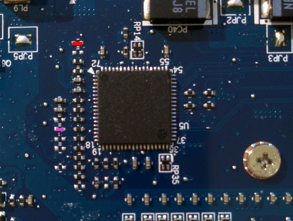
The modifications I made are nothing different than you, "electrically speaking". Both coloured marks are unused footprints for 402 smd devices. I have verified that the left pads of both 402 smd are connected to GND. - On the red footprint, the right pad is straightly routed to pin2 of the PLL chip (it can be verified on the system board schematic, p16). - The right pad of the pink footprint is connected to a 22 ohm resistor (the device at the right hand side of the mark), which is connected to the TME pin of the PLL. The only remaining thing to do is to short both pins of each footprint using an iron and some solder. No resistor to add, no wire... Very simple ! Anyway, thanks for the link, I will revert the mod on pin2 and try software overclocking using the file you shared. One more question : do you know why is clock multiplier locked to x6 when pin2 tied to GND ?
-
Hi Nando4, I lot of things have changed in my HP Elitebook 2530p lately. This last month, the L9600-based mainboard I used for the last 6 month has stopped charging battery... now, this same mainboard discharges batteries in few minutes. Since schematics avalaible for this system doesn't include the charging circuitry, the only remaining choice was to put another mainboard. So, today, I managed to replace it with an unused U9300 (1,2GHz) system board. Everything works well now, battery charges, etc.... Except that performances are really not the same. I read about the mod you proposed here and in NBR. I found a similar hardware mod solution (I find it slightly simpler) to pull down FLSB2 and TME pins of the PLL, see the red and pink shunts shown in the photo below : The red one is for shunting the pin2 of the PLL to GND. It changes the FSB freq. from 200 to 266 MHz. The pink mark is for the TME-unlock. Since I'm under linux, I would like to try the tricks using lfsb-ics9lprs397.tgz but the link is private. Is it possible for you to share this file with me ?

-
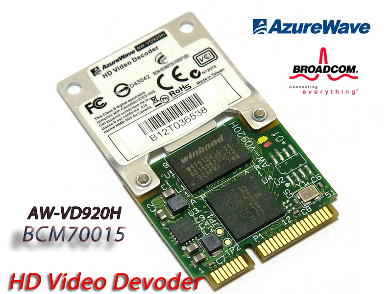
CrystalHD BCM70015 in an Elitebook 2530p ?
Xtof replied to Xtof's topic in HP Business Class Notebooks
Well, I answer to myself... This card works very well when placed in the WIFI mini-PCIe port. The WWAN mini-PCIe port is definitely whitelisted. I installed linux drivers and made a couple of tests (I'm using Ubuntu 13.04). I was hoping a drastic reduction of CPU occupation. It is better than the integrated intel GPU but bot outstandly exciting. Bad idea... -
Hi all, The CrystalHD BCM70015 is an hardware HD decoder. I may want to put it within laptop. Does anybody has tried this mod ? The 2530p has an available mini-PCIe port when no WWAN card is installed. I used this port to connect a CrystalHD BCM70015 but the card is not detected within bios and consecutively by the OS (Linux here). I suspect a whitelist blocking thing... My 2530p owns an F13 bios unwhitelisted by Tech Inferno Fan but maybe it is only for WLAN cards ? I will try to put this card in the WLAN port. Christophe

-
An AFFS LCD panel into the Elitebook 2530p Laptop
Xtof replied to Xtof's topic in HP Business Class Notebooks
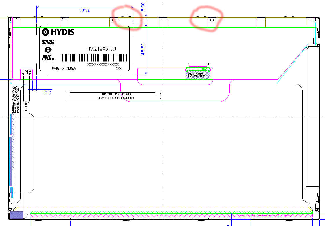
One last thing to do : Stock LCD panel dimensions are 178,0 x 275,8 mm² to be compared with the 180,0 x 276,8 mm² of the HV121WX5 panel. The 2nd one being 1mm larger, there is a little misalignment between the apertures of both hinges brackets and the back cover. when all of that is screwed, the edges of the back cover bend out. The apertures of the hinges brackets must be widened and the part of it touching the corner of back cover have to be smoothed. After that, the sceen fits in its cover like slippers at home ! -
Hi Nando4, Do you know if anyone has succeeded in reverting a > F20 BIOS to F13 for the 2530p ? I have 2 mainboards with socketed BIOS chips. One with the F12 version, and the other with the F21 version. I prefer ask before breaking something. Thanks !
-
An AFFS LCD panel into the Elitebook 2530p Laptop
Xtof replied to Xtof's topic in HP Business Class Notebooks
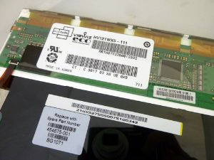
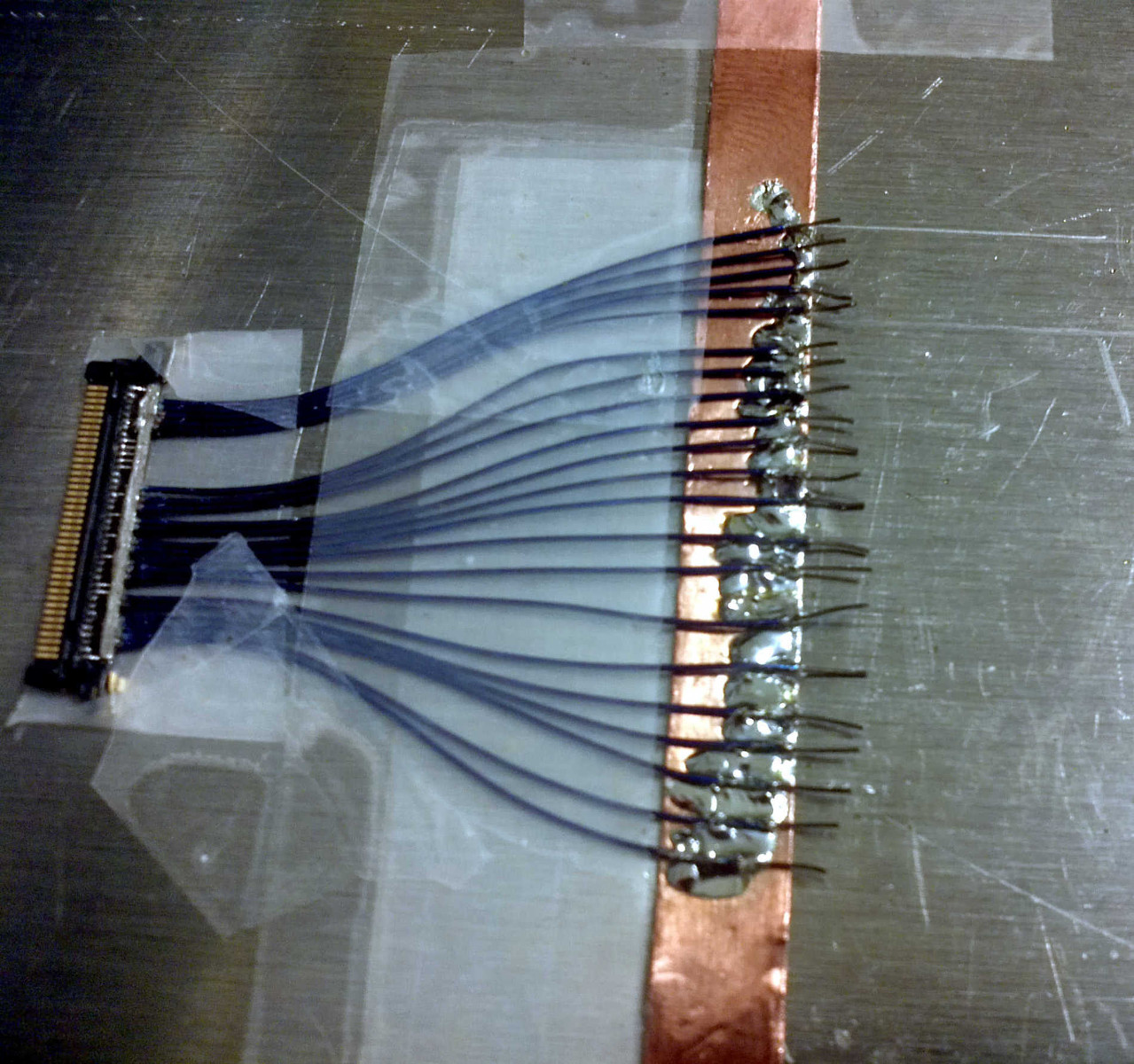
Thank you Nando4 for your comment. I'm glad you like this work. I will try to give some details of the thinning here. Unfortunately, I didn't took some pics during the process. OK. So yes, the HV121WX5-110 is really cheapper than the HV121WX6-XXX. It has a buit-in digitizer on the back, and a protective glass panel glued (around 1 mm thick) to the front side of LCD panel. With the used panels that can be found on ebay for example, this protective glass layer is often striped and imo, that's why it can be found at such low price. The trick here is that since we need to remove this glass layer, the LCD panel underneath is like a new one ! This is the good new. The bad new is now. Here is a pick of the back side of the panel : (The upper side of the LCD panel is the top of the pic) A close-up of the upper left part (The digitizer has been removed here) : From that pic, one can see the plastic white hooks that maintain the metal frame between each flexible PCB ribbons. On this side of the metal frame, the thickness is 6.5 mm. It must be refined to around 5,0 mm (like stock panel). If that part of the frame is not refined, it may cut the underneath WLAN and WLAN cables over time... Once it is refined to the right thickness, the plastic white hooks of this side are also cut. The LCD panel is a sandwitch of several layers. If the metal frame cannot hold them together, it may be a path for dust to go between LCD panel and backlight layer. I will see over time... The last part of the metal frame to cut is shown here (see the red circles) : This is because the global dimentions of the LCD are slightly higher than stock panels. Well, I did not expect such a proposal. I'm not planning to build other cables, maybe one more just in case mine breaks. It was a huge work that required a lot of time and attention. I did that only for fun, a sort of challenge. Frankly, it is not economically viable. You have to buy the cables. Considering shipping fees, I spent around 20€ for both. When you add the 10 hours or more in front of the binocular microscope.... What do you mean by "gone into Edit Power Plan" ? In fact, I have three mainboards and I can build 2 fully functionnal 2530p. The testing is only done on the second one. I don't want to break my business laptop. Yesterday, the first tests were done using the 1.6GHz L9300 mainboard which has a stock F12 BIOS. brightness adjustments never worked. Then I assembled the second mainboard, based on the 1.2 GHz U9300 CPU. This has a F21 BIOS version. Brightness adjustments have worked just fine unless I use the LS-402CP light sensor board to enable this functionality. I got some odd results that I don't yet understand. So I managed to put the new screen in my business laptop, based on the 2.13GHz L9600 CPU with F21 BIOS. Brightness adjustments work fine, but there is always this light sensor board issue. Well, it not a real problem, this functionality is, for me, just a gadget. But I still want to undrestand what is going on. So, I have the following assumptions : - Brightness adjustment is dead on the 1.6GHz L9300 mainboard (I doubt about that, I own this board since the beginning and it has never failed) - this is a BIOS version related issue. The 40pins LCD panels have been introduced lately during the 2530p life. I noticed that the later LED-based panels can work with PWM signal from 200 to 1 kHz. The HV121WX5 accepts PWM signal from only 200 to 350 Hz (see datasheet p7). So, I need to do further tests. OK, I will have a look at this topic to see if I can help. Thank you for that. Your 2530p pdf has only 36 pages, just like mine. It seems that there are some missing pages in it as explained here : Elitebook 2530p LA-4021p Full schematic - Power components • Forum ELVIKOM The LS-402CP data can be found there : Schemat HP EliteBook 2530p Compal LA-4021P SKYY • Forum ELVIKOM I tried to get some points to be able to download the "small board.rar" file without any success.

-
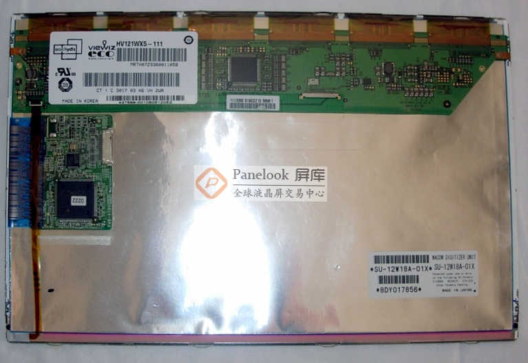
An AFFS LCD panel into the Elitebook 2530p Laptop
Xtof posted a topic in HP Business Class Notebooks
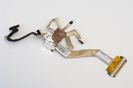
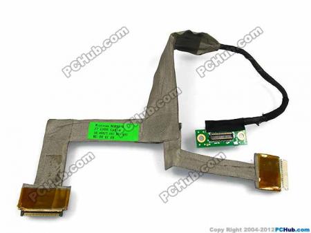
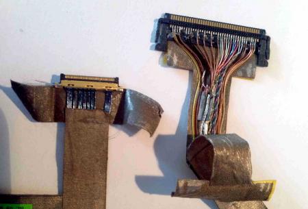
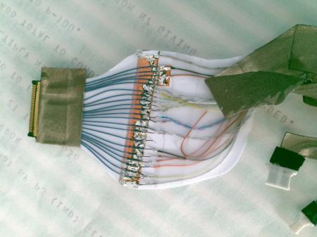
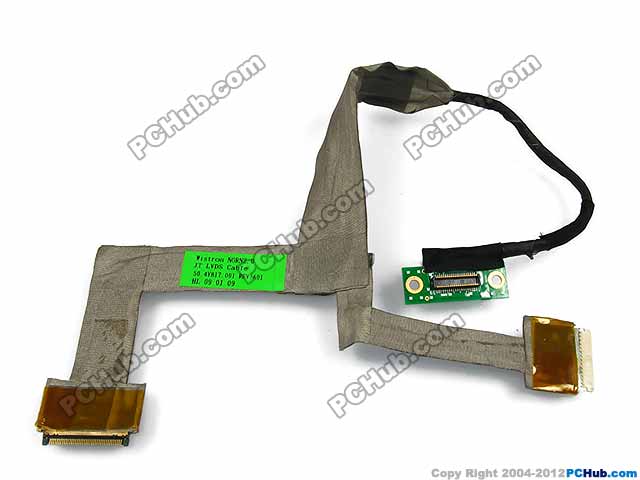
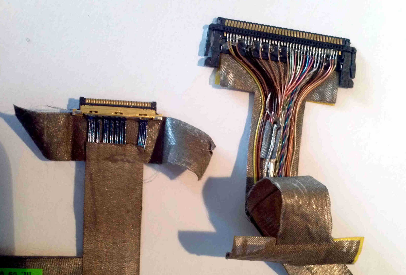
Hi there,This is my first post. I own a 2530p laptop since 2009. This is my "swiss army knife" computer. I use it every days at and off work.Since the begining, I'm bored with the poor quality of the stock screen. Recently, I decided to put a new one... and it is now almost working.Initially, I started this thread on NBR. I also was interested by the mod bioses proposed by Nando. Being unable to download it, and when I saw all that ban story, I decided to move everything here. So, let's continue here.Since none of the stock panels are very interesting, this modding will not be as simple as just a plug and play replacement. I spent a lot of time to understand the differents panels and options that come with the 2530p. I came to understand that there are basically four different panel assemblies. For each assembly, a different LCD cable can be bought. These are : PN conn. type Webcam DC02000LZ00 20 no DC02000JM00 20 yes DC02000WE00 40 no DC02000WF00 40 yes All the 20pins panels have an inverter outside the panel. The 40pins seems to be dedicated to the LED based LCD panel. I found that the following panels can be encountered inside 2530p laptops (+ maybe others) : manufacturer ref. viewing angles luminance contrast ratio con. type Samsung B121EW07 40/40/20/40 200 cd/m² 400:1 20 pins + 7pins Toshiba B121EW09 V2 30/30/10/20 200 cd/m² 500:1 40 pins The last one seems to be the only 40pins LCD panel that I found to be sold with some 2530p. Panel names on this table are linked to their respective datasheet. The good new is that the interface connector type and pinout is always fully described ! I think the best candidate is the AFFS Hydis HV121WX5-110 Hydis N121I7-L01 85/85/85/85 220 cd/m² 800:1 40 pins This screen is also found in HP 2710p and 2730p laptops. It may be a much better replacement (MVA type, better contrast), but it seems that the inverter is not built-in (or it is an error inside datasheet since it is a 40pins connector with LED backlight). This one is much harder to find and much more expensive too. Its 40pins connector is the same than hydis one but pinout is slightly different. The S-PVA Samsung LTN121AP03-001 display may be another good candidate, but I wasn't able to find any datasheet.So, I think the best candidate is still the HV121WX5-110 (AFFS type). In fact, any HV121WX5-XXX are OK, the last three numbers are only for a different manufacturing batch of the same panel.15th June 2013 I bought a DC02000WF00 2530p LCD cable and a 50.4Y817.001 rev A01 LCD cable that fits 2730p laptop. I received them yesterday. The goal is to use the the 2530p's cable with the 2730p LCD connector. Here are the two cables : The 2530p DC02000WF00 The 2730p 50.4Y817.001 [ATTACH=CONFIG]9300[/ATTACH] [ATTACH=CONFIG]9301[/ATTACH] some quite simple reverse engineering using a multimeter and the 2530p schematic (found